
NX15 Module Integration Overview
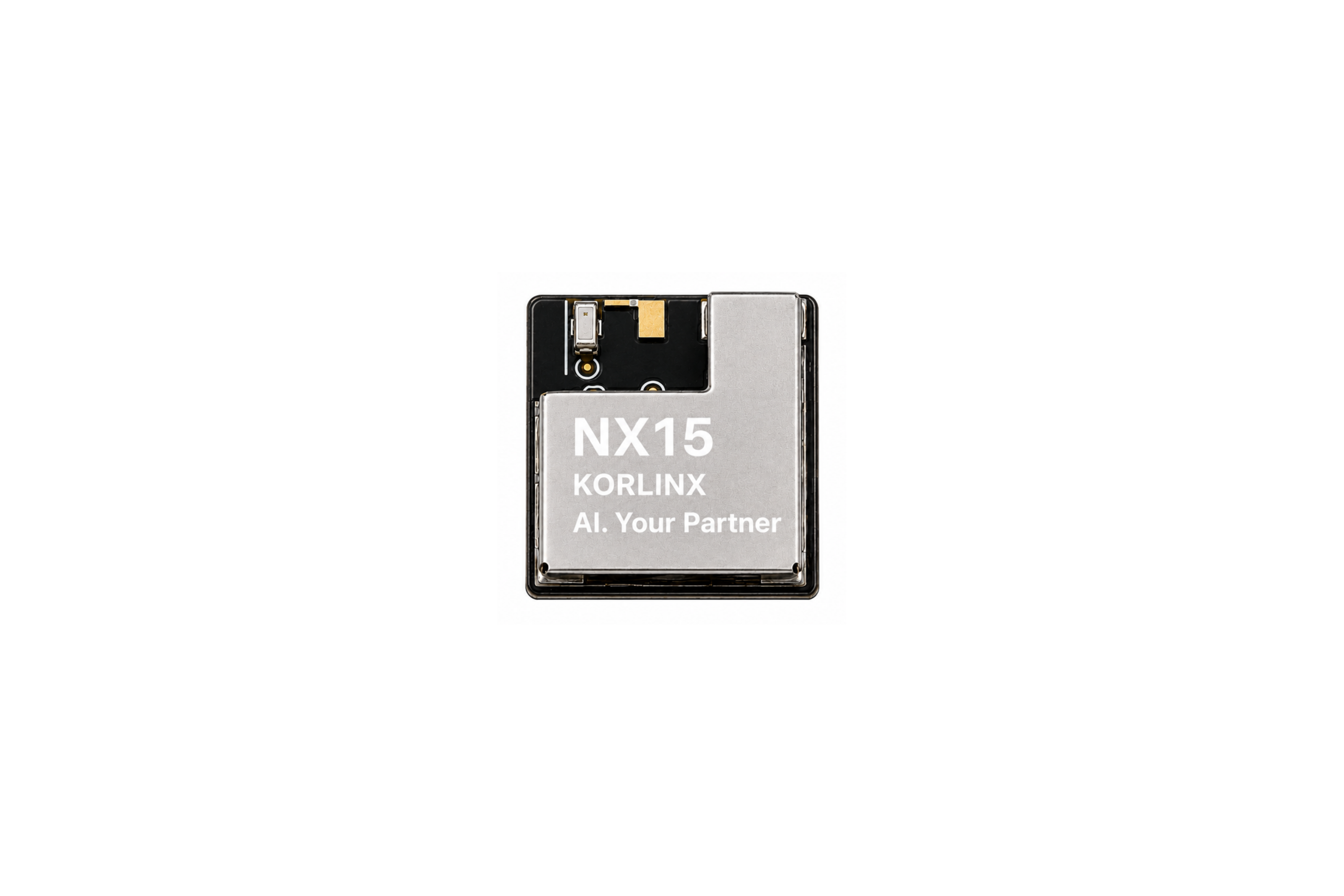
This section is for developers and hardware engineers who integrate the NX15 module into a custom PCB or host system.
It focuses on practical module-level integration topics such as model selection, PCB integration, LGA pad layout, handling, soldering, and bring-up troubleshooting.
note
This section is not a product introduction page. For general product information, see the NX15 Series BLE Module documentation.
Who Should Read This Section?
Read this section if you are:
| User Type | Goal |
|---|---|
| Hardware engineer | Integrate NX15 into a custom PCB |
| Firmware engineer | Understand available pins, debug access, and board constraints |
| Production engineer | Prepare SMT assembly, handling, and reflow process |
| System integrator | Validate power, antenna, programming, and bring-up path |
Integration Flow
Use the pages in this order:
| Step | Page | Purpose |
|---|---|---|
| 1 | Model Selection | Choose the correct NX15 variant |
| 2 | PCB Integration | Plan power, ground, debug, GPIO, and host connection |
| 3 | LGA Pad Layout | Understand pad groups and signal usage |
| 4 | Handling & Soldering | Prepare storage, assembly, reflow, and inspection |
| 5 | FAQ | Check common integration issues |
Integration Scope
This section covers:
| Topic | Covered Here |
|---|---|
| Model selection | Yes |
| Custom PCB integration | Yes |
| LGA pad usage | Yes |
| SMT handling and soldering | Yes |
| Basic integration troubleshooting | Yes |
| BLE application design | No |
| Thread / Matter application design | No |
| General Bluetooth introduction | No |
What This Section Does Not Replace
This section does not replace:
- The official datasheet
- Product-specific firmware guide
- RF validation report
- Production test procedure
- Certification test documentation
Use this section as the practical integration guide before moving to board-level validation.