
NX15 PCB Integration
This page provides a practical checklist for integrating the NX15 module into a custom host PCB.
It focuses on board-level integration. Detailed LGA pad usage is covered in NX15 LGA Pad Layout, and assembly handling is covered in NX15 Handling & Soldering.
PCB Integration Flow
| Step | Action |
|---|---|
| 1 | Select the NX15 model |
| 2 | Place the module on the host PCB |
| 3 | Connect power and ground |
| 4 | Add required decoupling capacitors |
| 5 | Route SWD programming/debug pins |
| 6 | Route reset and required GPIO |
| 7 | Check antenna area or u.FL RF path |
| 8 | Add test points for bring-up |
| 9 | Review manufacturing and reflow requirements |
| 10 | Validate the first prototype |
Module Placement
Place the module so that power, debug, GPIO, and antenna constraints can be satisfied.
| Area | Recommendation |
|---|---|
| PCB edge | Preferred for chip antenna variants |
| Antenna area | Keep clear according to antenna layout rules |
| Debug access | Keep SWD pins accessible |
| Test points | Add test points for VDD, GND, reset, and debug |
| Mechanical area | Avoid placing metal or battery too close to antenna area |
Power and Ground
| Signal / Area | Recommendation |
|---|---|
| VDD_nRF | Use a stable 1.7–3.6 V supply |
| GND | Connect every GND pad to a solid ground plane |
| Decoupling | Place 100 nF + 1 µF capacitors close to each VDD pad |
| Return path | Keep ground return path short and low impedance |
| Power test point | Add a VDD test point for bring-up measurement |
Do not power the first prototype before checking VDD/GND continuity and confirming that no power rail is shorted.
Programming and Debug Access
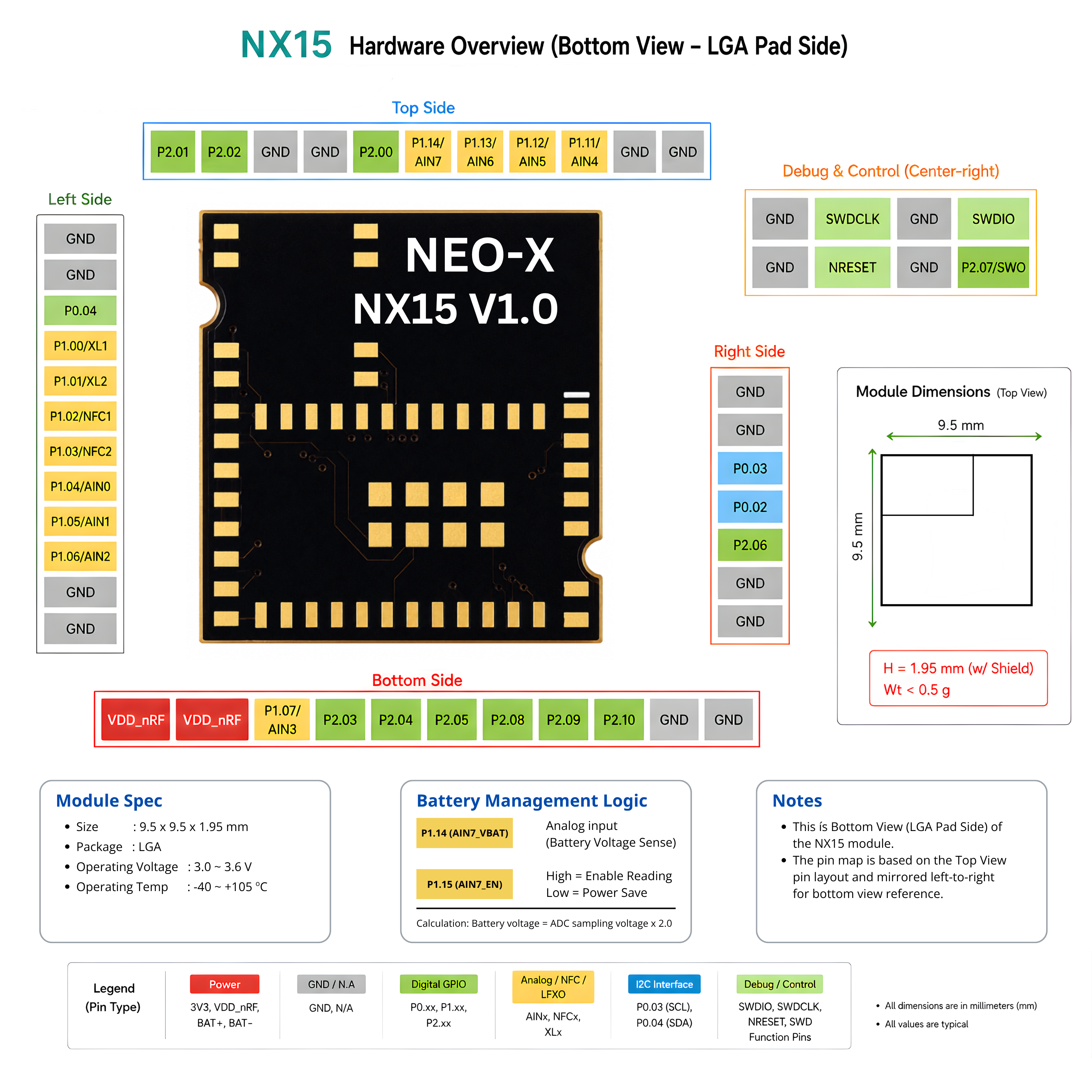
Keep SWD access available during development and production.
| Signal | Purpose | Recommendation |
|---|---|---|
| SWDIO | Programming/debug data | Route to header or test pad |
| SWDCLK | Programming/debug clock | Route to header or test pad |
| NRESET | Reset control | Route to button, header, or test pad |
| GND | Debug reference | Include near SWD pins |
| VDD sense | Target voltage reference | Add if required by debugger |
Even if the final product does not expose a debug connector, test pads are recommended for flashing, recovery, and production programming.
GPIO and Peripheral Routing
NX15 GPIO pins can be assigned to different peripheral functions through firmware configuration.
| Interface | Routing Note |
|---|---|
| UART | Confirm TX/RX direction and voltage level |
| SPI | Keep clock and data routing clean, especially at higher speed |
| I2C | Add pull-up resistors as required by the bus design |
| PWM | Check output load and drive requirements |
| ADC | Keep analog traces away from noisy or high-speed traces |
| PDM | Keep clock/data routing short and clean |
| GPIO | Confirm active level, pull-up/pull-down, and wake-up behavior |
Do not finalize GPIO routing before checking the firmware pin assignment and model variant constraints.
Antenna Integration Reminder
This page does not repeat full antenna rules, but antenna constraints must be checked before PCB release.
| Variant | Required Check |
|---|---|
| NX15i | Chip antenna keep-out and PCB edge placement |
| NX15E | u.FL connector, 50 Ω RF trace, and solid GND reference |
For full details, see the NX15 antenna design page in the NX15 Series BLE Module section.
Bring-up Test Points
Add test points for early validation.
| Test Point | Purpose |
|---|---|
| VDD_nRF | Verify supply voltage |
| GND | Measurement reference |
| SWDIO | Programming/debug |
| SWDCLK | Programming/debug |
| NRESET | Reset and recovery |
| UART TX/RX | Optional log or host communication |
| Key GPIO | Application-specific validation |
First Prototype Checklist
Before firmware testing:
| Check | Status |
|---|---|
| Correct NX15 model mounted | ☐ |
| VDD_nRF voltage is correct | ☐ |
| All GND pads are connected | ☐ |
| Decoupling capacitors are placed correctly | ☐ |
| SWDIO / SWDCLK are accessible | ☐ |
| NRESET is accessible | ☐ |
| Antenna layout is reviewed | ☐ |
| No visible soldering defect | ☐ |
| Current limit is set during first power-on | ☐ |