
NX15 Dev Kit Hardware
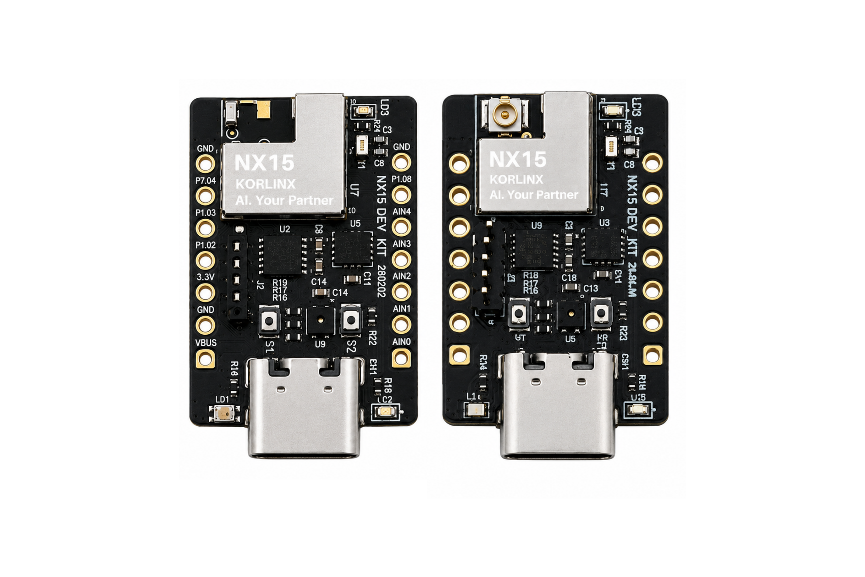
The NX15 Dev Kit provides the board-level hardware required to evaluate and develop applications with the KORLINX NX15 Series BLE module.
This page focuses on the Dev Kit hardware: USB connection, debugging interface, onboard sensors, buttons, LEDs, expansion headers, battery support, and the J3/J5 header pin map.
This page describes the NX15 Dev Kit board.
For module-level information such as LGA pad layout, antenna design, electrical/RF specifications, tape and reel packing, and soldering conditions, refer to the NX15 Module pages.
Hardware Overview
The NX15 Dev Kit combines the NX15 Series BLE module with development-friendly hardware so that users can test firmware, sensors, user input/output, serial communication, and external signal access more easily.
| Block | Contents | Purpose |
|---|---|---|
| Core Module | NX15 Series BLE module | Main wireless and processing module used on the Dev Kit |
| USB & Debugging | USB Type-C, FTDI FT234XD, SWD header, ESD/TVS protection | PC connection, serial communication, firmware programming, and debugging |
| LED & Switch | RGB LED, charge/power LEDs, reset button, user button | Firmware status indication and user input testing |
| Sensors | LSM6DS3TR-C 6-axis IMU, SHTC3 temperature/humidity sensor | Motion, orientation, temperature, and humidity example development |
| Headers | J3 and J5 headers | Selected signal access for prototyping and external connection |
| Battery Support | Li-Po connector, BQ25100 charger IC | Battery-oriented BLE prototype testing |
Dev Kit Specification
| Item | Specification |
|---|---|
| Product | NX15 Dev Kit |
| Target Module | KORLINX NX15 Series BLE module |
| Main SoC | Nordic nRF54L15 |
| Wireless | Bluetooth LE 5.4 |
| Multiprotocol Support | 802.15.4 capable: Thread / Zigbee |
| Matter Support | Matter over Thread capable depending on software stack |
| CPU | 128 MHz Arm Cortex-M33 |
| Coprocessor | 128 MHz RISC-V coprocessor |
| Internal Memory | 1.5 MB internal NVM, 256 KB RAM |
| External Flash | Optional external Flash depending on NX15 module model |
| RF Output Power | TX up to +8 dBm |
| Development Interface | USB Type-C |
| USB-to-UART | FTDI FT234XD |
| Debug Interface | SWD header |
| On-board Sensors | LSM6DS3TR-C 6-axis IMU, SHTC3 temperature/humidity sensor |
| Buttons | Reset button, user button |
| LEDs | RGB LED, charge LED, power LED |
| Expansion Headers | J3 and J5 headers |
| Battery Hardware | Li-Po connector, BQ25100 charger IC |
| Development Platform | nRF Connect SDK / Zephyr RTOS compatible |
The module-level values in this table describe the NX15 module used on the Dev Kit. They should not be used as a replacement for the full NX15 module datasheet during custom PCB design.
Key Features
- Development-ready board: Provides the essential hardware needed to evaluate the NX15 Series BLE module.
- USB Type-C connection: Allows convenient PC connection for development and testing.
- USB-to-UART interface: Uses FTDI FT234XD for serial communication during development.
- SWD debugging: Provides SWD access for programming, debugging, and firmware validation.
- Onboard sensors: Includes LSM6DS3TR-C 6-axis IMU and SHTC3 temperature/humidity sensor for example applications.
- User input and status output: Provides reset/user buttons, RGB LED, charge LED, and power LED.
- Expansion headers: Exposes selected module signals through J3 and J5 headers for prototyping.
- Battery-oriented prototyping: Includes Li-Po connector and BQ25100 charger IC for battery-related test workflows.
USB and Debugging
The NX15 Dev Kit includes USB and debugging hardware for firmware development, serial communication, and board bring-up.
| Hardware | Purpose |
|---|---|
| USB Type-C | Main PC connection during development |
| FTDI FT234XD | USB-to-UART communication interface |
| SWD header | Firmware programming and debugging interface |
| ESD / TVS protection | Protection for USB and external interface areas |
Use the USB Type-C connector for normal development connection. Use the SWD header when firmware programming, debugging, or recovery access is required.
Sensors, Buttons, and LEDs
The Dev Kit includes onboard sensors and user interface components for quick firmware validation.
| Hardware | Purpose |
|---|---|
| LSM6DS3TR-C | 6-axis motion sensing for motion and orientation examples |
| SHTC3 | Temperature and humidity sensing for environmental examples |
| RGB LED | Firmware-controlled status or application indicator |
| Charge LED | Battery charging status indication |
| Power LED | Board power status indication |
| Reset Button | Resets the board or target module |
| User Button | General-purpose user input for firmware examples |
Headers and Battery Support
The NX15 Dev Kit provides expansion headers and battery-related hardware for prototype development.
| Hardware | Purpose |
|---|---|
| J3 header | Selected signal access for external connection and testing |
| J5 header | Selected signal access for external connection and testing |
| Li-Po connector | Battery-powered prototype testing |
| BQ25100 charger IC | Li-Po battery charging support |
This allows the board to be used for both USB-powered development and battery-oriented BLE prototype testing.
Pin Map
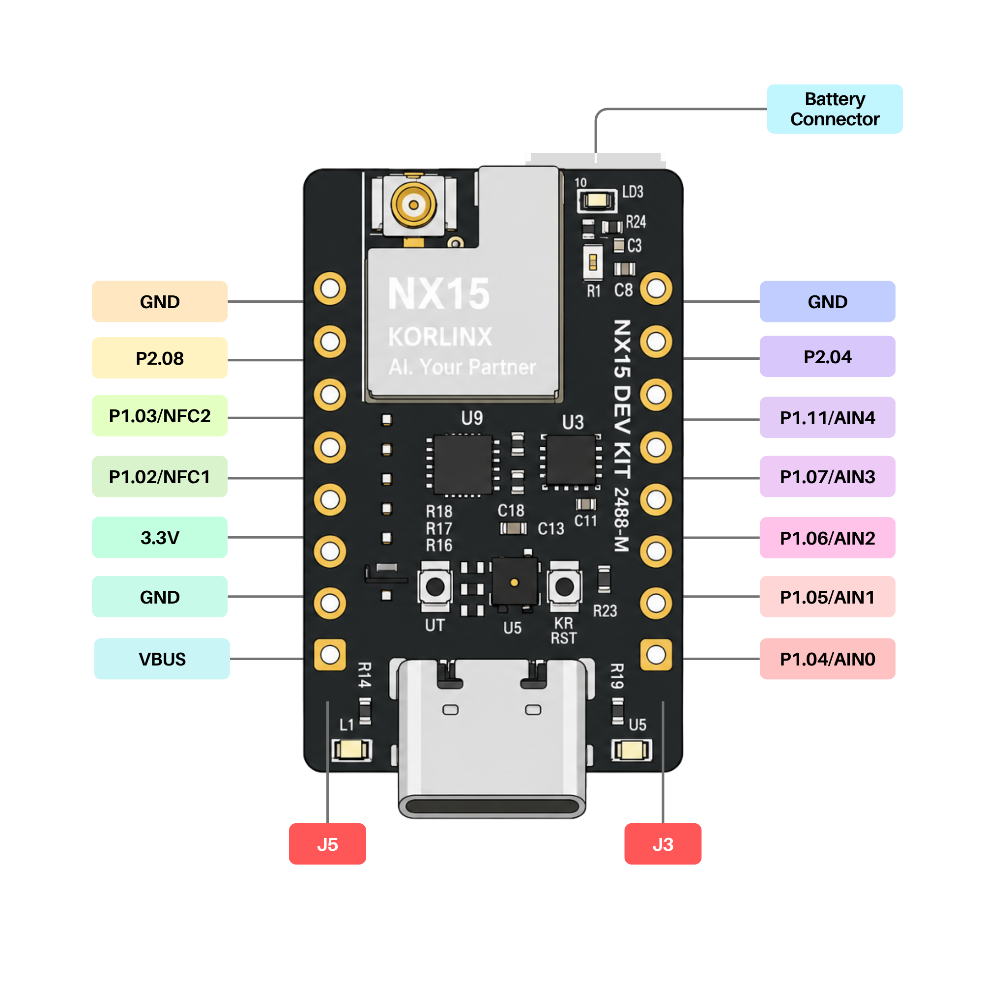
The NX15 Dev Kit exposes selected NX15 module signals through the J3 and J5 header areas. These headers can be used for prototyping, external sensor connection, GPIO testing, and firmware validation.
This pin map shows the NX15 Dev Kit J3/J5 header signals.
It is not the full NX15 module LGA pad map. For the full module pad map, refer to the NX15 Module Pin Map page.
J5 Header
| Pin Order | Pin Label | Type | Description |
|---|---|---|---|
| 1 | GND | Ground | Common ground reference |
| 2 | P2.08 | GPIO / Trace | General-purpose I/O or trace-related alternate function |
| 3 | P1.03 / NFC2 | GPIO / NFC | GPIO or NFC2 antenna interface |
| 4 | P1.02 / NFC1 | GPIO / NFC | GPIO or NFC1 antenna interface |
| 5 | 3.3V | Power | 3.3 V board power rail reference |
| 6 | GND | Ground | Common ground reference |
| 7 | VBUS | Power | USB bus voltage input |
J3 Header
| Pin Order | Pin Label | Type | Description |
|---|---|---|---|
| 1 | GND | Ground | Common ground reference |
| 2 | P2.04 | GPIO / SPI / QSPI | General-purpose I/O, SPI/QSPI-capable alternate function |
| 3 | P1.11 / AIN4 | GPIO / ADC | GPIO or analog input channel AIN4 |
| 4 | P1.07 / AIN3 | GPIO / ADC | GPIO or analog input channel AIN3 |
| 5 | P1.06 / AIN2 | GPIO / ADC | GPIO or analog input channel AIN2 |
| 6 | P1.05 / AIN1 | GPIO / ADC | GPIO or analog input channel AIN1 |
| 7 | P1.04 / AIN0 | GPIO / ADC | GPIO or analog input channel AIN0 |
Pin Usage Notes
| Item | Note |
|---|---|
| Header pin map | The J3/J5 tables describe selected Dev Kit header signals only |
| Module LGA pad map | The full NX15 module LGA pad map is documented separately in the NX15 Module Pin Map page |
| GPIO function | GPIO and peripheral functions depend on firmware configuration |
| NFC pins | NFC-related pins may require firmware configuration before use as GPIO |
| ADC pins | Analog input routing should be kept away from noisy or high-speed traces |
| Production design | Confirm the final Dev Kit schematic and NX15 module datasheet before production use |
Hardware Use Cases
| Use Case | Example |
|---|---|
| BLE sensor demo | Use onboard sensors to build BLE environmental or motion data examples |
| Button and LED test | Validate user input and firmware status indication |
| Serial communication test | Use USB-to-UART for logs, commands, or serial data exchange |
| Debugging and firmware validation | Use SWD access for programming and debugging |
| External sensor prototype | Connect external signals through J3/J5 headers |
| Battery-oriented prototype | Test BLE application behavior with Li-Po battery-related hardware |
Need Confirmation from Korean Technical Team
The following items should be confirmed before final public release:
| Item | Why Confirmation Is Needed |
|---|---|
| Final Dev Kit schematic | Confirms the official board-level connection of USB, FTDI, SWD, sensors, buttons, LEDs, headers, and battery circuit |
| J3/J5 header mapping | Confirms that the published header pin map matches the final Dev Kit hardware |
| Power rail description | Confirms whether 3.3V and VBUS should be described as output, input, or reference pins in the final Wiki |
| Battery workflow | Confirms the approved description for Li-Po connector and BQ25100 charging behavior |
| Software workflow | Confirms whether only nRF Connect SDK / Zephyr RTOS should be shown, or whether Arduino-related content will be added later |