
NX15 Module Pin Map
This page describes the external LGA pad map of the KORLINX NX15 Series BLE module.
The NX15 module exposes selected power, ground, reset, debug, GPIO, NFC, ADC, SPI, QSPI, trace, and configurable peripheral signals through its external LGA pads.
This page describes the NX15 module LGA pad map.
For the NX15 Dev Kit J3 / J5 header pin map, see the NX15 Dev Kit Hardware page.
LGA Pad Layout
The NX15 module uses an LGA package for surface-mount integration. The external pads provide access to the main power, ground, debug, reset, GPIO, and configurable peripheral functions.
For production PCB design, always confirm the final pad assignment with the official datasheet, schematic, and engineering release documents.
System, Power, and Debug Pins
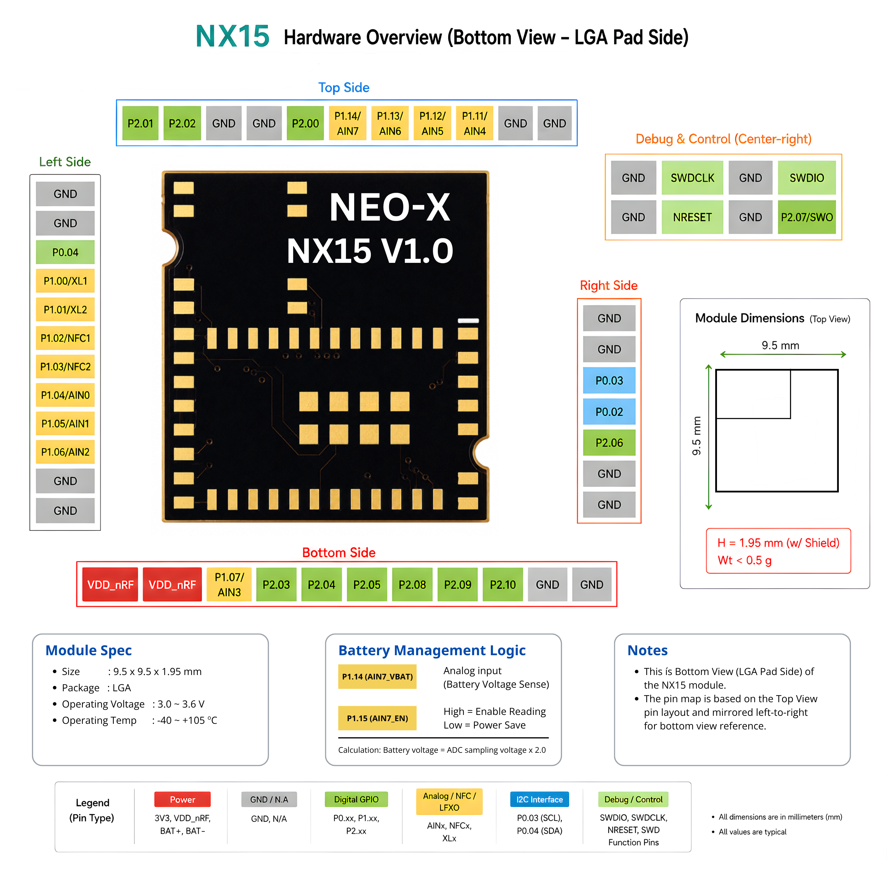
| Pad / Signal | Type | Nordic CSP47 Ball | Function | Design Note |
|---|---|---|---|---|
| VDD_nRF | Power | B7, G3 | Main module supply | Use nominal 3.3 V and place decoupling capacitors close to each VDD pad |
| GND | Ground | Module GND plane | Ground, including radio-supply ground | Connect every external GND pad to a solid ground plane with short vias |
| NRESET | Reset | D2 | Pin reset with on-chip pull-up | Route to a reset button and/or debug connector; keep accessible for bring-up and recovery |
| SWDIO | Debug | F2 | Serial wire data | Route to an SWD header or test pad |
| SWDCLK | Debug | E3 | Serial wire clock input with on-chip pull-down | Route with SWDIO and keep the trace short |
Keep reset and SWD access available during early bring-up. This helps firmware programming, debugging, and device recovery.
GPIO and Configurable Peripheral Signals
NX15 GPIO pins can be assigned to different peripheral functions depending on firmware configuration.
Typical functions include:
| Function Group | Example Use |
|---|---|
| GPIO | General digital input/output |
| UART / UARTE | Host communication or serial peripheral connection |
| SPI / SPIM / SPIS | Sensors, memory, or high-speed peripheral interface |
| QSPI | External memory or high-speed interface depending on configuration |
| I2C | Sensor or low-speed peripheral interface |
| PWM | LED, buzzer, or control output |
| ADC / AIN | Analog sensor input |
| PDM | Digital microphone interface |
| NFC | NFC antenna function when enabled |
| Trace / SWO | Debug trace function |
GPIO and peripheral functions are configurable by firmware. Do not assume that a pad is available for user GPIO without checking the final firmware configuration, model option, and schematic.
P0 GPIO Pins
| Signal | Nordic CSP47 Ball | Function | Design Note |
|---|---|---|---|
| P0.00 | G1 | General-purpose digital I/O | Confirm the firmware and model-specific assignment before use |
| P0.01 | F1 | General-purpose digital I/O | Confirm the firmware and model-specific assignment before use |
| P0.02 | E2 | General-purpose digital I/O | Confirm the firmware and model-specific assignment before use |
| P0.03 | E1 | General-purpose digital I/O; GRTC PWM | Clock-capable; confirm the firmware and model-specific assignment before use |
| P0.04 | D3 | General-purpose digital I/O; GRTC CLKOUT32K | Clock-capable; confirm the firmware and model-specific assignment before use |
NFC and Analog Input Pins
Some NX15 pads can support NFC or analog input functions depending on firmware configuration.
| Signal | Nordic CSP47 Ball | Alternate Signals | Design Note |
|---|---|---|---|
| P1.00 / XL1 | C5 | GPIO / XL1 | Use as an LFXO crystal pin when an external 32.768 kHz crystal is required; otherwise firmware may assign it as GPIO |
| P1.01 / XL2 | C6 | GPIO / XL2 | Use as an LFXO crystal pin when an external 32.768 kHz crystal is required; otherwise firmware may assign it as GPIO |
| P1.02 / NFC1 | C7 | GPIO / NFC1 | Keep as NFC1 when NFC is required; confirm GPIO availability in firmware when NFC is disabled |
| P1.03 / NFC2 | D5 | GPIO / NFC2 | Clock-capable; keep as NFC2 when required and confirm GPIO availability when NFC is disabled |
| P1.04 / AIN0 | D6 | GPIO / ASO[0] / AIN0 | Keep analog routing away from noisy or high-speed traces |
| P1.05 / AIN1 | E6 | GPIO / ASI[0] / RADIO[6] / AIN1 | RADIO DFEGPIO use requires firmware/radio configuration |
| P1.06 / AIN2 | D7 | GPIO / ASO[1] / AIN2 | Keep analog routing away from noisy or high-speed traces |
| P1.07 / AIN3 | E7 | GPIO / ASI[1] / AIN3 | Keep analog routing away from noisy or high-speed traces |
| P1.11 / AIN4 | C4 | GPIO / ASO[3] / RADIO[2] / AIN4 | Clock-capable; add input protection or filtering as required |
| P1.12 / AIN5 | A3 | GPIO / ASI[3] / RADIO[3] / AIN5 | Clock-capable; add input protection or filtering as required |
For analog sensing, keep analog input routing away from noisy or high-speed traces. Add input protection or filtering when required by the sensor interface.
P2 GPIO / SPI / QSPI / Trace Pins
Several P2 pins support configurable GPIO, SPI, QSPI, UARTE, or trace-related functions.
| Signal | Nordic CSP47 Ball | Alternate Signals | Design Note |
|---|---|---|---|
| P2.00 | G6 | GPIO / SPIM DCX / UARTE RXD / FLPR.4 / QSPI D3 | Confirm availability before use; see the source comment below |
| P2.01 | G7 | GPIO / SPIM SCK / SPIS SCK / FLPR.0 / QSPI SCK | Clock-capable; use short, direct routing for high-speed SPI/QSPI |
| P2.02 | F6 | GPIO / SPIM SDO / SPIS SDO / UARTE TXD / FLPR.1 / QSPI D0 | Confirm availability before use; see the source comment below |
| P2.03 | E5 | GPIO / FLPR.3 / QSPI D2 | Confirm availability before use; see the source comment below |
| P2.04 | F5 | GPIO / SPIM SDI / SPIS SDI / UARTE CTS / FLPR.2 / QSPI D1 | Confirm availability before use; see the source comment below |
| P2.05 | G5 | GPIO / SPIM CSN / SPIS CSN / UARTE RTS / FLPR.5 / QSPI CSN | Confirm availability before use; see the source comment below |
| P2.06 | F4 | GPIO / FLPR.6 / SPIM SCK / SPIS SCK / TRACECLK | Use short routing for high-speed SPI or trace clock |
| P2.07 / SWO | E4 | GPIO / FLPR.7 / TRACEDATA[0] / SWO / SPIM DCX / UARTE RXD | Primarily a debug trace/SWO pad; GPIO-capable when SWO is unused |
| P2.08 | D4 | GPIO / FLPR.8 / TRACEDATA[1] / SPIM SDO / SPIS SDO / UARTE TXD | Available for GPIO or peripheral use when trace is unused |
| P2.09 | F3 | GPIO / FLPR.9 / TRACEDATA[2] / SPIM SDI / SPIS SDI / UARTE CTS | Available for GPIO or peripheral use when trace is unused |
| P2.10 | G2 | GPIO / FLPR.10 / TRACEDATA[3] / SPIM CSN / SPIS CSN / UARTE RTS | Available for GPIO or peripheral use when trace is unused |
PCB Design Rules
Follow these general rules when designing a host PCB for the NX15 module:
- Connect all GND pads to a solid ground plane.
- Place 100 nF and 1 µF bypass capacitors near each VDD pin.
- Maintain the required RF keep-out area around the antenna edge.
- Keep debug access available during development.
- Confirm all model-specific pin usage before finalizing the PCB.
Important Pin Usage Notes
| Item | Note |
|---|---|
| Firmware-configurable pins | GPIO and peripheral functions depend on firmware configuration |
| Internal module functions | Some SoC pins are handled internally by the module and are not available as external user pads |
| External Flash models | Pin availability and internal Flash usage may differ depending on model |
| SWO / Trace | P2.07 / SWO is debug trace-capable and should be treated carefully in production designs |
| RF and crystal pins | RF, 32 MHz crystal, regulator decoupling, and DC/DC-related pins are handled internally by the module |
Module-Internal Pins
These nRF54L15 signals are handled inside the NX15 module and are not routed as external user pads.
| CSP47 Ball | nRF54L15 Signal | Internal Use |
|---|---|---|
| A1 | XC1 | Internal 32 MHz crystal connection |
| A2 | XC2 | Internal 32 MHz crystal connection |
| D1 | ANT | Internal antenna path: chip antenna on NX15i or u.FL path on NX15E |
| A4 | DECA | Internal regulator-supply decoupling |
| B1 | DECRF | Internal radio-supply decoupling |
| A5 | DECD | Internal regulator-supply decoupling |
| A7 | DCC | Internal DC/DC regulator output |
| C2 | VSS_PA | Internal radio-supply grounding |