
NX15 Module Specifications
This page summarizes the main specifications of the KORLINX NX15 Series BLE module.
It is intended as a quick reference for developers and hardware engineers before reviewing the detailed pin map, antenna, and handling pages.
:::note Specification sources NX15-specific RF, current, and voltage measurements are not available. Values identified as SoC specifications come from the Nordic nRF54L15 Product Specification; they are not measured or guaranteed NX15 module values. Use released KORLINX engineering documents for production design. :::
Key Specifications
| Item | Specification |
|---|---|
| Product Series | NX15 Series |
| Product Type | Bluetooth Low Energy module |
| Main SoC | Nordic nRF54L15 |
| CPU | 128 MHz Arm Cortex-M33 |
| Coprocessor | 128 MHz RISC-V coprocessor |
| Internal Memory | 1.5 MB internal NVM, 256 KB RAM |
| External Flash | Optional external Flash depending on model |
| Wireless | Bluetooth LE 5.4 |
| 802.15.4 Support | Thread / Zigbee capable |
| Matter Support | Matter over Thread capable depending on software stack |
| RF Output Power | Up to +8 dBm for the nRF54L15 CSP package (SoC specification) |
| RX Sensitivity | −96 dBm, Bluetooth LE 1 Mbps (SoC specification) |
| Operating Supply Range | 1.7 V to 3.6 V; maximum 3.4 V under extended-temperature conditions (SoC specification) |
| Operating Temperature | −40°C to +85°C; extended operation to +105°C under Nordic's specified conditions (SoC specification) |
| Power Regulation | Integrated DC-DC and LDO regulators |
| Package | LGA surface-mount module |
| Module Size | 9.5 × 9.5 × 1.95 mm |
| Module Weight | < 0.5 g |
| Pad Pitch | 0.65 mm |
| Interfaces | UART, SPI, I2C, PWM, ADC, PDM, GPIO, SWD |
| SDK / RTOS | nRF Connect SDK / Zephyr RTOS |
| Security | Arm TrustZone and nRF54L15 platform security features |
Selecting a Model
The antenna and additional-Flash combinations are summarized once on the NX15 Module Overview. After selecting a model, use this page to check the shared electrical, RF, mechanical, memory, and interface specifications.
For antenna-specific integration requirements, continue to the NX15 Module Antenna page.
Mechanical Information
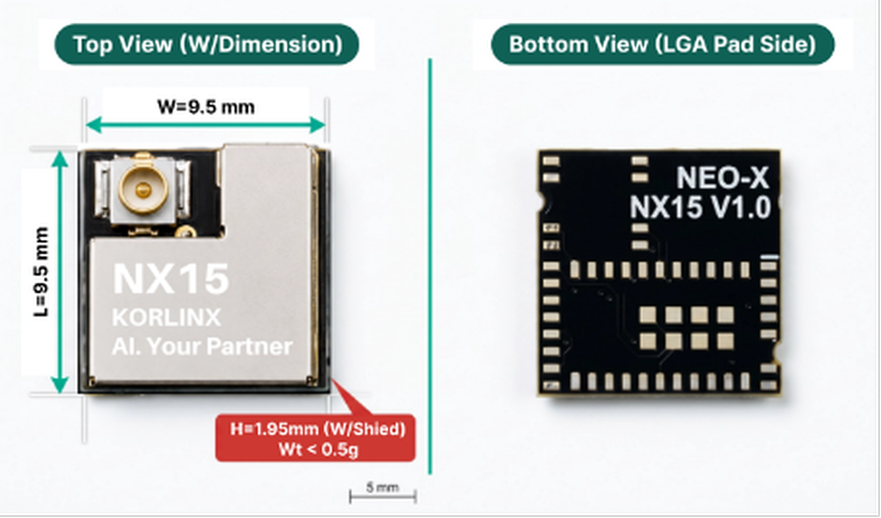
| Parameter | Value | Note |
|---|---|---|
| Length | 9.5 mm | Module body |
| Width | 9.5 mm | Module body |
| Height | 1.95 mm | With shield |
| Weight | < 0.5 g | Typical target |
| Package | LGA | Surface-mount module |
| Pad Pitch | 0.65 mm | Landing pattern reference |
SoC Absolute Maximum Ratings
These are nRF54L15 CSP-package limits from the Nordic product specification. They are stress limits, not NX15 operating conditions or module qualification results.
| Parameter | Symbol | Minimum | Maximum | Unit | Source scope |
|---|---|---|---|---|---|
| Supply voltage | VDD | −0.3 | 3.9 | V | nRF54L15 SoC |
| GPIO voltage, VDD ≤ 3.6 V | VIO | −0.3 | VDD + 0.3 | V | nRF54L15 SoC |
| RF input level | — | — | 10 | dBm | nRF54L15 SoC |
| Storage temperature | TSTG | −40 | +125 | °C | nRF54L15 CSP package |
| Reflow temperature | TREFLOW | — | 260 | °C | nRF54L15 CSP package; 30 seconds, maximum three cycles |
| ESD, Human Body Model | — | — | 3 | kV | nRF54L15 CSP package |
SoC Recommended Operating Conditions
| Parameter | Symbol | Minimum | Typical | Maximum | Unit |
|---|---|---|---|---|---|
| Supply voltage | VDD | 1.7 | — | 3.6 | V |
| Supply voltage, extended temperature | VDD_EXT | 1.7 | — | 3.4 | V |
| Operating temperature | TA | −40 | 25 | +85 | °C |
| Extended operating temperature | TA_EXT | +85 | — | +105 | °C |
| GPIO Input High Voltage | VIH | 0.7 × VDD_nRF | - | VDD_nRF | V |
| GPIO Input Low Voltage | VIL | GND | - | 0.3 × VDD_nRF | V |
| GPIO High-Level Output | VOH | VDD_nRF - 0.4 | - | VDD_nRF | V |
| GPIO Low-Level Output | VOL | GND | - | GND + 0.4 | V |
| GPIO Output Current, Standard Drive | IGPIO_SD | - | - | 0.5* | mA |
| GPIO Output Current, High Drive | IGPIO_HD | - | 3 | 5* | mA |
* GPIO output current depends on VDD_nRF, drive-strength configuration, load conditions, and firmware settings. Standard-drive output is specified at a 0.5 mA load. High-drive output current is typically 3 mA at VDD_nRF ≥ 1.7 V and up to 5 mA at VDD_nRF ≥ 2.7 V.
Nordic SoC Electrical, RF, and Current Reference
The following values are from the Nordic nRF54L15 Product Specification. They describe the SoC under Nordic's stated conditions and are not NX15 module measurements. Unless a row says otherwise, Nordic's current-consumption conditions use 3 V on VDD, 25°C, and the reference circuit; regulator, clock, and memory conditions depend on the selected scenario.
| Item | Typical / Range | Unit | Nordic condition |
|---|---|---|---|
| Arm Cortex-M33 Clock | 128 | MHz | 128 MHz Arm Cortex-M33 |
| RISC-V Coprocessor Clock | 128 | MHz | 128 MHz RISC-V coprocessor |
| Internal NVM | 1.5 | MB | Internal NVM |
| RAM | 256 | KB | RAM |
| External Flash | Optional | - | Depending on model |
| Frequency Band | 2402–2480 | MHz | BLE 5.4 |
| Maximum TX output power | +8 | dBm | CSP package |
| Bluetooth LE RX sensitivity | −96 | dBm | 1 Mbps PHY |
| IEEE 802.15.4 RX sensitivity | −102 | dBm | 250 kbps PHY |
| Radio TX current | 6.6 | mA | +4 dBm, HFXO |
| Radio TX current | 9.8 | mA | +8 dBm, HFXO |
| Radio RX current | 3.4 | mA | 1 Mbps, HFXO |
| System OFF current | 0.7 | µA | Wake on pin, 0 KB RAM retained |
| System ON idle current | 2.9 | µA | Wake on pin + GRTC/LFXO, 256 KB RAM retained |
See Nordic's radio current table and sleep-current table for definitions and test conditions.
Interface Summary
NX15 provides configurable embedded interfaces for host communication, sensor connection, peripheral control, programming, and debugging.
| Interface | Available Resources | Typical Use |
|---|---|---|
| UART / UARTE | 2 | Host communication or serial peripheral connection |
| SPI | 3, including SPI up to 32 MHz | External sensors, memory, or high-speed peripheral connection |
| I2C | 2 | Sensor or low-speed peripheral connection |
| PWM | 4 | LED, buzzer, control, or signal output |
| ADC | 8 channels | Analog input for external sensors |
| PDM | 1 | Digital microphone interface |
| GPIO | P0, P1, and P2 ports | General digital input/output |
| SWD | SWDIO and SWDCLK | Programming and debugging |
GPIO and peripheral functions are configurable by firmware. Confirm the final pin assignment, firmware configuration, and model-specific restrictions before using a pin in a custom design.