
NX40 Quick Start
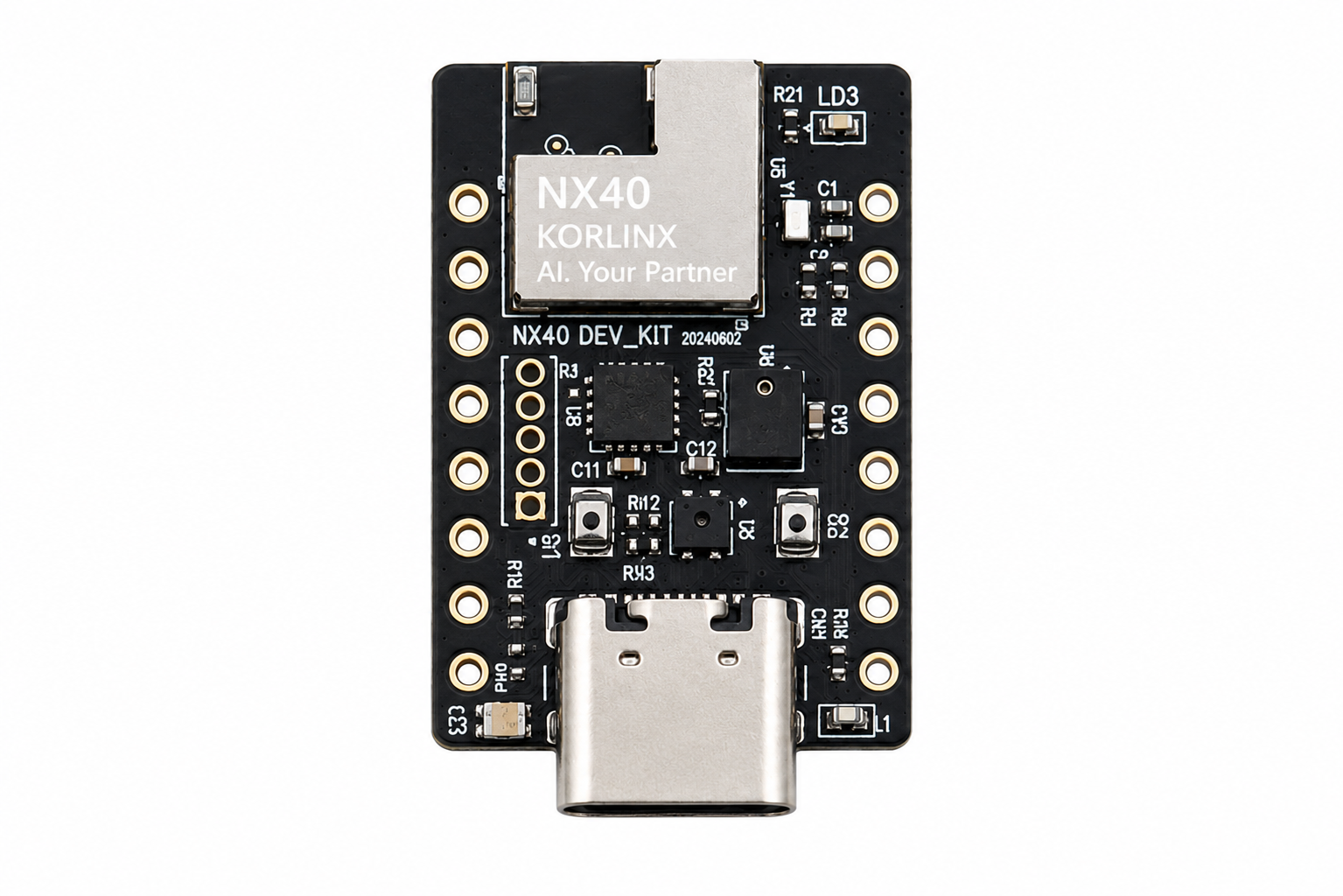
This guide helps you bring up the NX40 Series BLE module for the first time.
Use this page when you want to:
- Prepare an NX40-based board for first power-on
- Check the programming and debugging path
- Flash or run a basic firmware example
- Verify basic BLE advertising or wireless behavior
- Continue to hardware, antenna, low-power, and application development
This page focuses on the first bring-up flow. Detailed PCB layout, antenna rules, low-power tuning, and production handling are covered in separate pages to avoid duplicated content.
Quick Start Flow
| Step | Action | Expected Result |
|---|---|---|
| 1 | Select the NX40 variant | Antenna and Flash option match the project requirement |
| 2 | Prepare the hardware | NX40 board or custom PCB is ready |
| 3 | Check power path | Power rail is stable and safe for first bring-up |
| 4 | Prepare programming/debugging | SWDIO, SWDCLK, GND, and reset access are available |
| 5 | Prepare firmware environment | Build and flashing workflow is ready |
| 6 | Flash a basic firmware example | Firmware starts running on the board |
| 7 | Verify basic operation | LED, UART log, BLE advertising, or debug output is confirmed |
| 8 | Continue development | BLE, sensors, host interfaces, and low-power features can be added |
1. Select the NX40 Variant
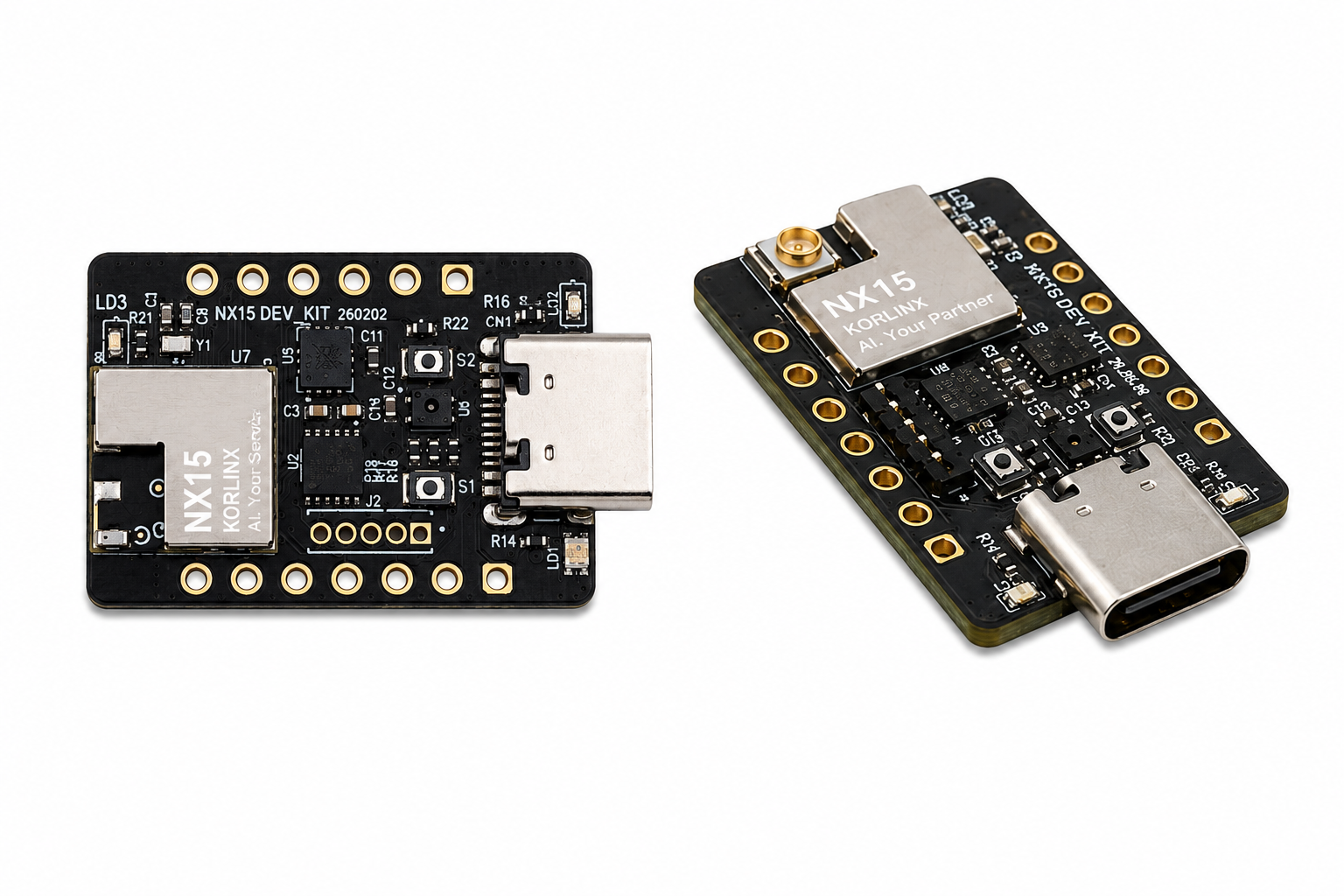
Choose the NX40 variant based on antenna type and external Flash requirement.
| Model | Antenna | Flash | Use When |
|---|---|---|---|
| NX40i32 | Chip antenna | 32 Mbit SPI Flash | You need chip antenna integration and external Flash |
| NX40E32 | u.FL external antenna | 32 Mbit SPI Flash | You need external antenna placement and external Flash |
| NX40i00 | Chip antenna | None | You need chip antenna integration without external Flash |
| NX40E00 | u.FL external antenna | None | You need external antenna placement without external Flash |
For early RF validation, use the same antenna type that your final product is expected to use.
2. Prepare the Hardware
There are two common bring-up paths.
Option A — NX40 Evaluation or Development Board
Use this path if NX40 is mounted on an evaluation or development board.
Check:
| Area | What to Confirm |
|---|---|
| Power input | Board receives stable power |
| Debug connector | SWD or programming path is available |
| Reset | Reset signal can be controlled |
| LEDs / buttons | Useful for first firmware validation |
| Antenna area | Antenna is not blocked by metal or the test setup |
Option B — Custom Host PCB
Use this path if NX40 is mounted directly on your own PCB.
| Area | What to Confirm |
|---|---|
| Power | Power rail is correct and stable |
| Ground | Ground path is continuous and low impedance |
| Debug | SWDIO / SWDCLK / GND / reset are accessible |
| Flash option | Firmware configuration matches the NX40 model |
| Antenna | Chip antenna area or u.FL RF path is implemented |
| Test points | Key bring-up signals are accessible |
Do not continue bring-up if the power path, debug path, or antenna layout is uncertain. Review the hardware and antenna design pages first.
3. Check Programming and Debug Access
Before flashing firmware, confirm the minimum debug signals.
| Signal | Purpose |
|---|---|
| SWDIO | Programming/debug data |
| SWDCLK | Programming/debug clock |
| GND | Common debug reference |
| RESET / NRESET | Reset and recovery |
| Target voltage reference | Allows debugger to detect target voltage, if required |
Keep debug access available during development. It is useful for flashing, debugging, board recovery, and production programming.
4. Prepare the Firmware Environment
NX40 firmware development should follow the board support package and project repository provided for the NX40 platform.
Prepare:
| Item | Purpose |
|---|---|
| SDK / firmware workspace | Build and application development |
| Board definition | Pin mapping and hardware configuration |
| Debug/programming tool | Firmware flashing and debugging |
| Serial terminal | Optional logs or test output |
| BLE scanner | Verify BLE advertising or connection behavior |
The exact board target, build command, and flashing command depend on the NX40 firmware repository or SDK package. Do not assume that a generic board target is correct.
5. Flash a Basic Firmware Example
Start with a simple firmware example before testing a full application.
Recommended first examples:
| Example Type | Purpose |
|---|---|
| LED blink | Confirms firmware is running |
| UART log | Confirms serial output path |
| Button input | Confirms input GPIO behavior |
| BLE advertising | Confirms BLE radio path |
| Basic sensor read | Confirms external sensor or peripheral path, if used |
Suggested bring-up sequence:
- Build a basic sample for the NX40 board target.
- Flash the firmware through the supported programming path.
- Reset the board.
- Confirm the expected LED, log, or BLE advertising behavior.
The board configuration must match the actual NX40 model, antenna option, external Flash option, and PCB pin routing.
6. Verify BLE Operation
For first wireless validation, start with BLE advertising.
| Check Item | Expected Result |
|---|---|
| Firmware starts | Application runs without reset loop |
| BLE advertising | Device appears in a BLE scanner |
| RSSI behavior | Signal changes when the scanner moves closer or farther |
| Antenna condition | Signal is stable in the intended orientation |
| Reboot behavior | Device starts reliably after reset or power cycle |
For RF comparison, keep the test setup consistent. Board orientation, antenna type, enclosure material, nearby metal, and test distance can all affect BLE signal behavior.
7. First Bring-up Checklist
Use this checklist before moving to application development.
| Item | Status |
|---|---|
| Correct NX40 variant selected | ☐ |
| Board or custom PCB prepared | ☐ |
| Power path confirmed | ☐ |
| SWD/programming path confirmed | ☐ |
| Reset path confirmed | ☐ |
| Firmware environment prepared | ☐ |
| Basic firmware flashed | ☐ |
| LED/log/basic output confirmed | ☐ |
| BLE advertising verified | ☐ |
Troubleshooting
Keep troubleshooting short on this page. Detailed hardware, antenna, and firmware issues should be handled in their dedicated pages or FAQ.
| Symptom | Possible Cause | Next Check |
|---|---|---|
| Board does not power on | Power or GND issue | Check power design and first power-on procedure |
| Cannot flash firmware | SWD or reset issue | Check SWDIO, SWDCLK, GND, reset, and target voltage |
| Firmware runs but no log | UART path or log configuration issue | Check board configuration and serial settings |
| BLE device not visible | Firmware, antenna, or RF setup issue | Check advertising sample and antenna design |
| Device resets unexpectedly | Power instability or firmware issue | Measure power during boot and radio activity |
| High current consumption | Firmware not entering sleep or peripherals active | Check Low Power Guide |
🎉 You're Ready!
Your NX40 bring-up path is ready
You've selected the NX40 variant, prepared the hardware, checked debug access, flashed a basic firmware example, and verified first BLE behavior.
From first power-on to BLE advertising — your NX40 project is ready for hardware validation and application development.
- ✅ Selected the correct NX40 variant
- ✅ Prepared the board or custom hardware
- ✅ Checked power and debug access
- ✅ Prepared the firmware development environment
- ✅ Flashed a basic firmware example
- ✅ Verified basic BLE operation
What's next?
Hardware Design
Review power, debug, reset, GPIO, and board-level design requirements.
Antenna Design
Check chip antenna placement or u.FL external antenna design.
Low Power Guide
Optimize sleep behavior, radio timing, and peripheral usage.
BLE Application
Start BLE advertising, connection, GATT services, or gateway-based workflows.
Your NX40 module is ready for the next stage: hardware validation, BLE application development, and low-power tuning.