
NX40 Dev Kit Hardware Overview
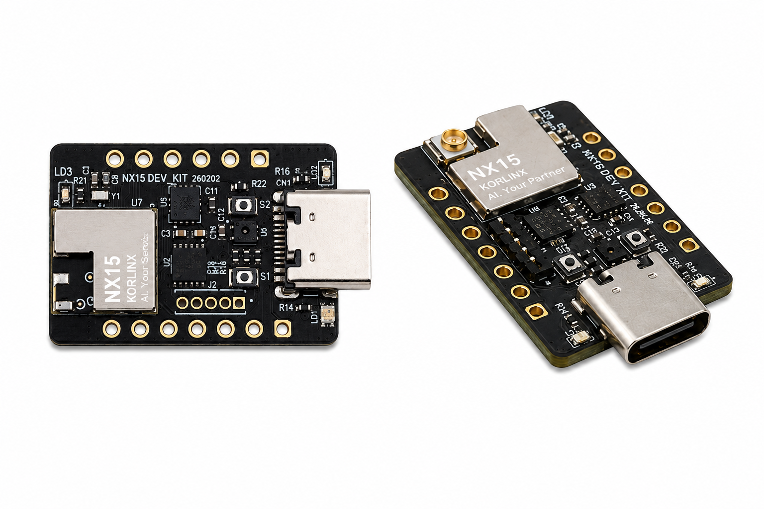
The KORLINX NX40 Dev Kit is a compact development board designed for evaluating, prototyping, and developing applications with the NX40 Series BLE module. The NX40 Series is intended for Bluetooth Low Energy and 2.4 GHz embedded applications such as BLE sensors, beacons, wearable devices, smart home devices, industrial monitoring nodes, and short-range wireless control systems.
The Dev Kit provides essential hardware for early development, including USB Type-C, FTDI USB-to-UART, SWD debugging, onboard LSM6DS3TR-C 6-axis IMU, SHTC3 temperature/humidity sensor, RGB LED, user/reset buttons, expansion headers, Li-Po connector, and battery charging support.
Hardware Overview
The NX40 Dev Kit includes USB connectivity, debugging access, user input, status output, onboard sensors, expansion headers, and battery-related hardware.
| Block | Contents |
|---|---|
| USB & Debugging | USB Type-C, FTDI FT234XD, SWD header |
| LED & Switch | RGB LED, charge/power LEDs, reset button, user button |
| Sensors | LSM6DS3TR-C 6-axis IMU, SHTC3 temperature/humidity sensor |
| Pins & Battery | J3 / J4 headers, Li-Po connector, BQ25100 charger IC |
Specification
| Item | Specification |
|---|---|
| Product | NX40 Dev Kit |
| Module Series | NX40 Series BLE Module |
| Wireless | Bluetooth Low Energy / 2.4 GHz embedded applications |
| Main Platform | nRF52840 platform |
| Module Models | NX40i32, NX40E32, NX40i00, NX40E00 |
| Antenna Options | Chip antenna for NX40i, external antenna for NX40E |
| External Flash | 32 Mbit SPI Flash or no external Flash depending on model |
| GPIO Summary | Counting policy pending module-level technical approval |
| Module Package | LGA surface-mount module |
| Module Size | 9.5 × 9.5 × 1.95 mm |
| Module Pad Pitch | 0.65 mm |
| Dev Kit USB Interface | USB Type-C |
| USB-to-UART | FTDI FT234XD |
| Debug Interface | SWD header |
| On-board Sensors | LSM6DS3TR-C 6-axis IMU, SHTC3 temperature/humidity sensor |
| Buttons | Reset button, user button |
| LEDs | RGB LED, charge/power LEDs |
| Expansion | J3 / J4 headers |
| Battery Support | Li-Po connector, BQ25100 charger IC |
| Software Platform | nRF Connect SDK / Zephyr RTOS workflow, subject to released board support and firmware verification |
Features
- Compact BLE Development Board: Provides a ready-to-use platform for evaluating and prototyping applications with the NX40 Series BLE module.
- Bluetooth Low Energy Platform: Designed for BLE sensors, beacons, wearable devices, smart home devices, industrial monitoring nodes, and short-range wireless control applications.
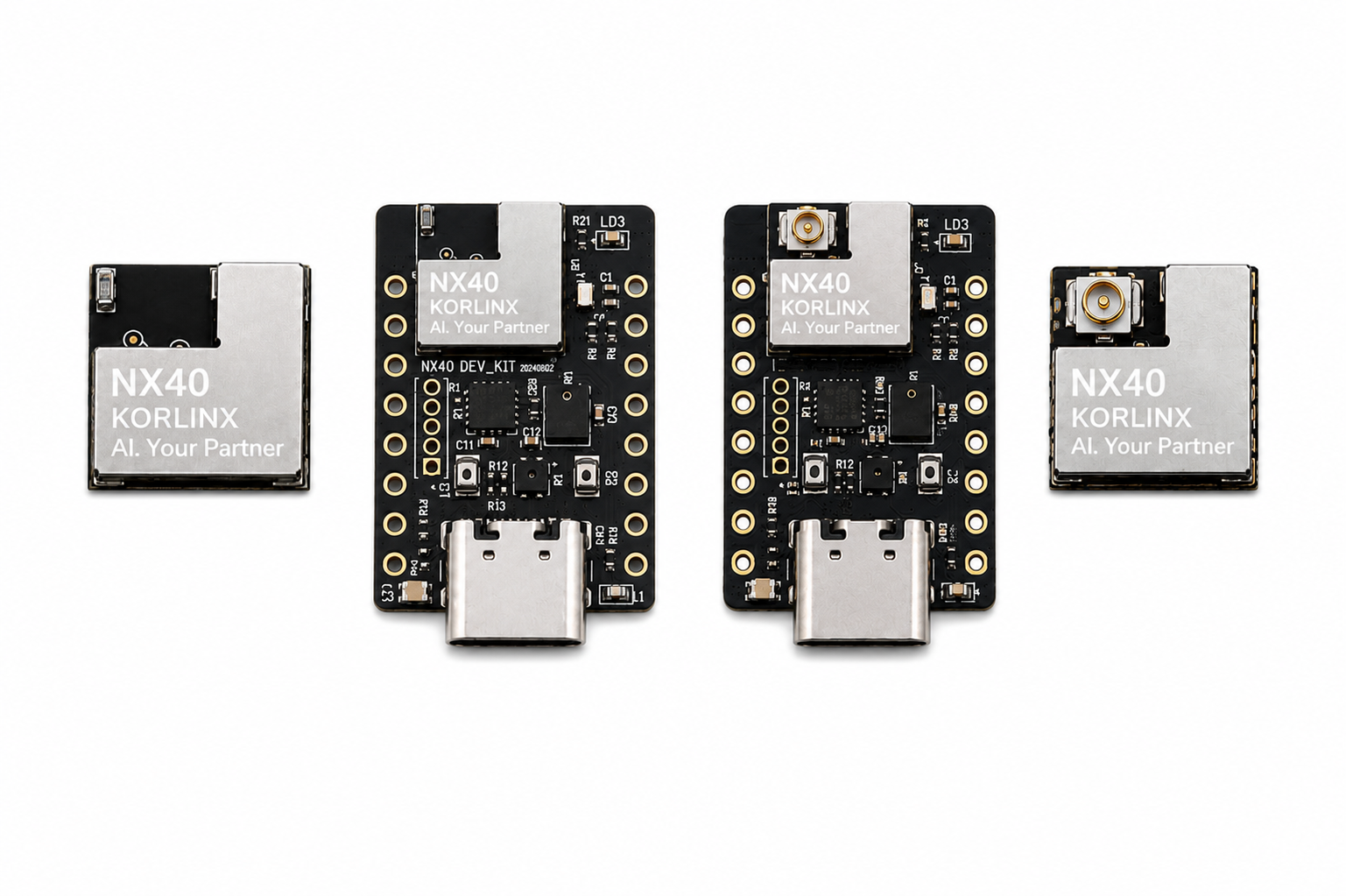
- NX40 Module Support: Supports NX40 chip antenna and external antenna variants, with Flash and no-Flash model options depending on the selected module.
- On-board Sensor Support: Includes an LSM6DS3TR-C 6-axis IMU and an SHTC3 temperature/humidity sensor for motion, orientation, and environmental sensing examples.
- Development-ready Hardware: Provides USB Type-C, FTDI FT234XD USB-to-UART, SWD debugging, RGB LED, charge/power LEDs, reset button, user button, J3/J4 headers, Li-Po connector, and BQ25100 charger IC.
- Zephyr-based Development: Compatible with the nRF Connect SDK and Zephyr RTOS development workflow.
Pin Map
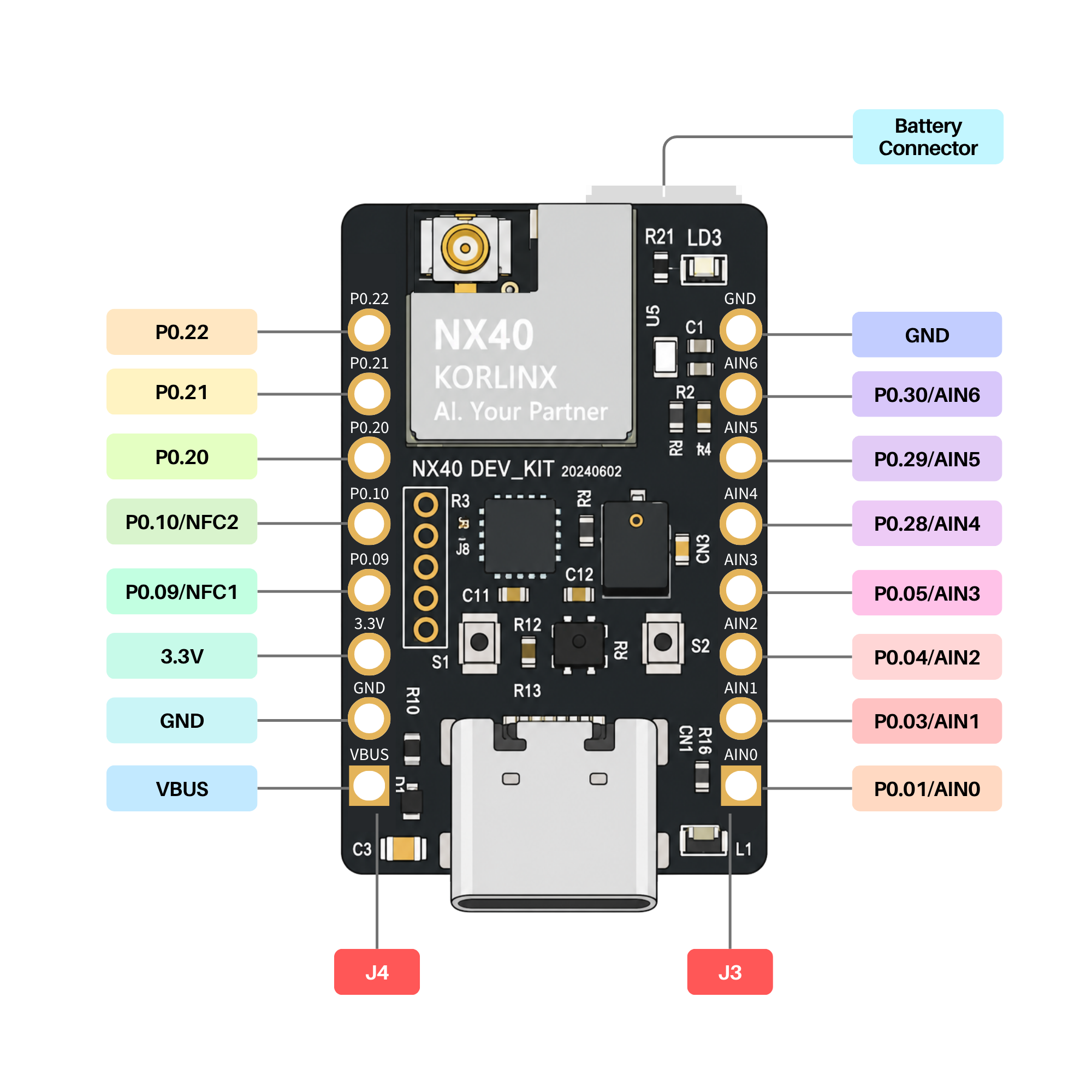
The NX40 Dev Kit exposes commonly used NX40 module signals through the J3 and J4 header areas. These pins can be used for prototyping, external sensor connection, GPIO testing, analog input testing, and firmware validation.
This pin map is based on the NX40 Dev Kit pin illustration. Always confirm the final header mapping with the official schematic before production use.
J4 Header
| Pin Order | Pin Label | Type | Description |
|---|---|---|---|
| 1 | P0.22 | GPIO | General-purpose I/O |
| 2 | P0.21 | GPIO | General-purpose I/O |
| 3 | P0.20 | GPIO | General-purpose I/O |
| 4 | P0.10 / NFC2 | GPIO / NFC | GPIO or NFC2 antenna interface |
| 5 | P0.09 / NFC1 | GPIO / NFC | GPIO or NFC1 antenna interface |
| 6 | 3.3V | Power | 3.3 V output / board power rail reference |
| 7 | GND | Ground | Common ground reference |
| 8 | VBUS | Power | USB bus voltage input |
J3 Header
| Pin Order | Pin Label | Type | Description |
|---|---|---|---|
| 1 | GND | Ground | Common ground reference |
| 2 | P0.30 / AIN6 | GPIO / ADC | GPIO or analog input channel AIN6 |
| 3 | P0.29 / AIN5 | GPIO / ADC | GPIO or analog input channel AIN5 |
| 4 | P0.28 / AIN4 | GPIO / ADC | GPIO or analog input channel AIN4 |
| 5 | P0.05 / AIN3 | GPIO / ADC | GPIO or analog input channel AIN3 |
| 6 | P0.04 / AIN2 | GPIO / ADC | GPIO or analog input channel AIN2 |
| 7 | P0.03 / AIN1 | GPIO / ADC | GPIO or analog input channel AIN1 |
| 8 | P0.01 / AIN0 | GPIO / ADC | GPIO or analog input channel AIN0 |
Pin Map Summary
| Header | Pins |
|---|---|
| J4 | P0.22, P0.21, P0.20, P0.10/NFC2, P0.09/NFC1, 3.3V, GND, VBUS |
| J3 | GND, P0.30/AIN6, P0.29/AIN5, P0.28/AIN4, P0.05/AIN3, P0.04/AIN2, P0.03/AIN1, P0.01/AIN0 |