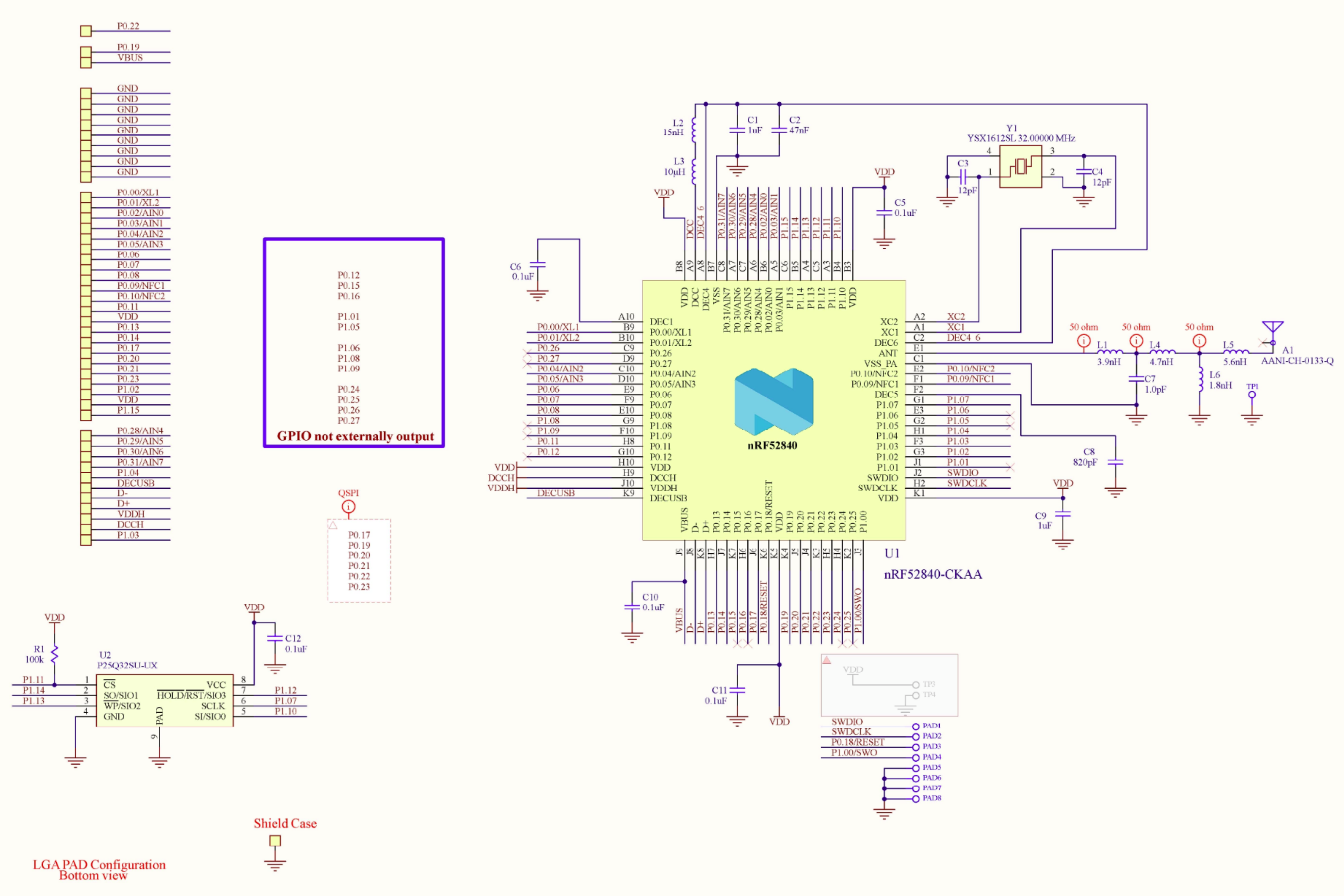
NX40 Module Pin Map
The NX40 LGA interface exposes power, ground, USB, debug, GPIO, analog, NFC, and trace-capable signals from the nRF52840 platform.
Design review required: The SoC ball names were checked against the nRF52840 product specification. The mapping from those balls to NX40 LGA pads is KORLINX design data and requires sign-off against the released PCB netlist and continuity test.
LGA Pad Layout
Power, USB, and Debug Signals
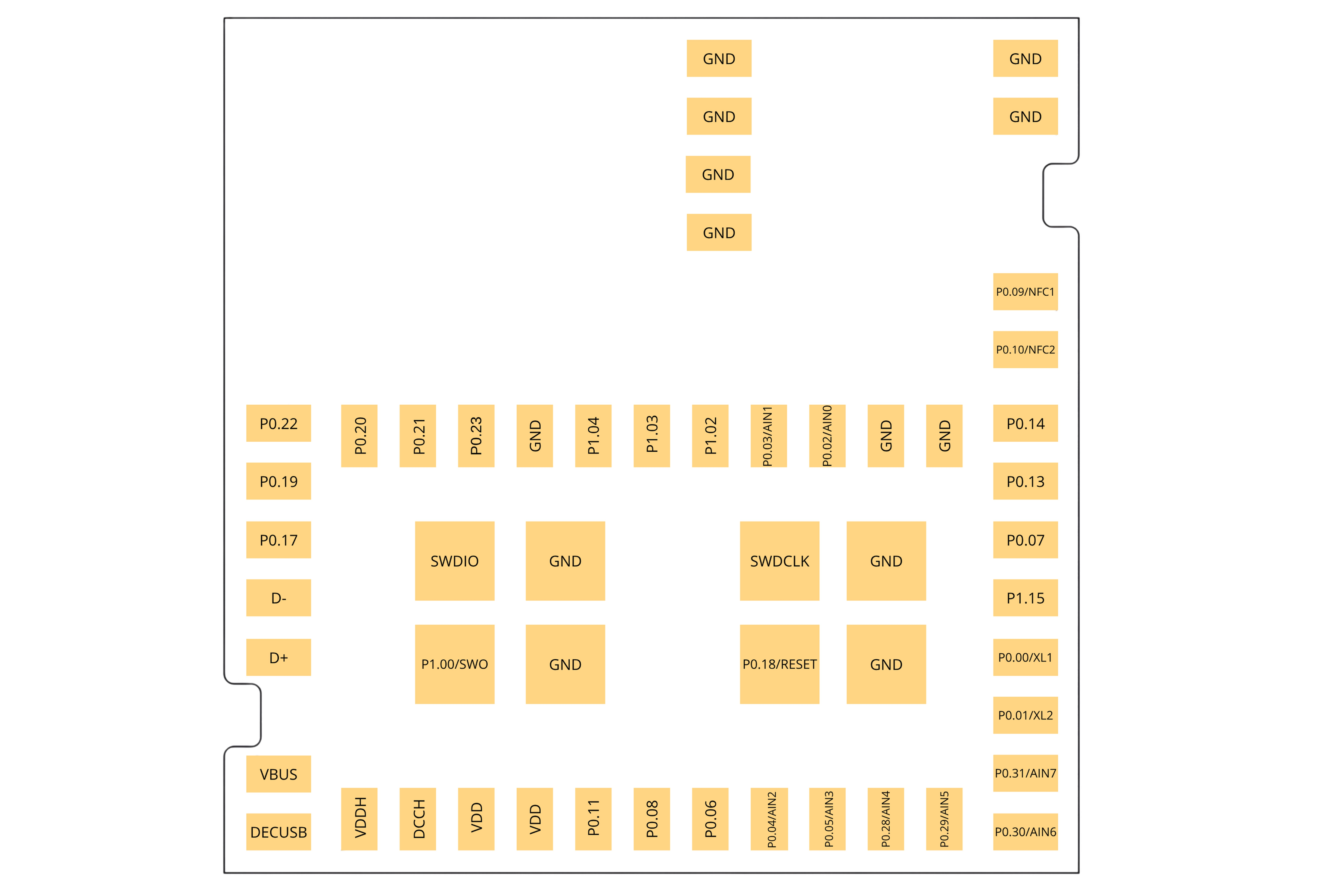
| Signal | WLCSP ball(s) | Primary role | Integration note |
|---|---|---|---|
| VDD | B3, B8, H10, K1, K5 | Normal-voltage supply | Connect external VDD pads to the approved rail and decoupling network |
| GND | Multiple VSS balls / module ground | Ground | Connect every module ground pad to a continuous ground plane |
| VDDH | J10 | High-voltage input | Use only with the approved high-voltage topology |
| DCCH | H9 | DC/DC node | Do not use as a general-purpose supply output |
| VBUS | J9 | USB supply input | Follow VDD/VDDH powering rules |
| DECUSB | K9 | USB regulator decoupling | Connect only the specified capacitor |
| D− / D+ | J8 / K8 | USB data | Route as a controlled 90 Ω differential pair |
| P0.18 / nRESET | K6 | GPIO / reset / QSPI CSN | Function depends on firmware configuration |
| SWDIO / SWDCLK | J2 / H2 | Programming and debug | Keep accessible for production programming and recovery |
Exposed GPIO-Capable Signals
| Group | Signals | Count |
|---|---|---|
| P0 regular, analog, and trace | P0.00, .01, .02, .03, .04, .05, .06, .07, .08, .11, .13, .14, .17, .19, .20, .21, .22, .23, .28, .29, .30, .31 | 22 |
| P0 special | P0.09/NFC1, P0.10/NFC2, P0.18/nRESET | 3 |
| P1 regular | P1.02, P1.03, P1.04, P1.15 | 4 |
| P1 special | P1.00/SWO | 1 |
| Total GPIO-capable external signals | Includes configurable special-function signals | 30 |
P0 Signal Map
| NX40 signal | WLCSP ball | Function summary |
|---|---|---|
| P0.00/XL1 | B9 | GPIO / LFXO |
| P0.01/XL2 | B10 | GPIO / LFXO |
| P0.02/AIN0 | B6 | GPIO / ADC |
| P0.03/AIN1 | A5 | GPIO / ADC |
| P0.04/AIN2 | C10 | GPIO / ADC |
| P0.05/AIN3 | D10 | GPIO / ADC |
| P0.06 | E9 | GPIO |
| P0.07/TRACECLK | F9 | GPIO / trace |
| P0.08 | E10 | GPIO |
| P0.09/NFC1 | F1 | GPIO / NFC |
| P0.10/NFC2 | E2 | GPIO / NFC |
| P0.11/TRACEDATA2 | H8 | GPIO / trace |
| P0.13 | H7 | GPIO |
| P0.14 | J7 | GPIO |
| P0.17 | J6 | GPIO |
| P0.19 | K4 | GPIO / QSPI SCK recommendation |
| P0.20 | J5 | GPIO |
| P0.21 | J4 | GPIO / QSPI recommendation |
| P0.22 | K3 | GPIO / QSPI recommendation |
| P0.23 | H5 | GPIO / QSPI recommendation |
| P0.28/AIN4 | A6 | GPIO / ADC |
| P0.29/AIN5 | C7 | GPIO / ADC |
| P0.30/AIN6 | A7 | GPIO / ADC |
| P0.31/AIN7 | C8 | GPIO / ADC |
P1 Signal Map
| NX40 signal | WLCSP ball | Use |
|---|---|---|
| P1.00/SWO | J3 | GPIO / trace / QSPI recommendation |
| P1.02 | G3 | External GPIO |
| P1.03 | F3 | External GPIO |
| P1.04 | H1 | External GPIO |
| P1.15 | C6 | External GPIO |
Module-Internal Flash Signals
On 32 variants, these signals connect to the additional serial Flash and are not exposed as customer LGA signals.
| Signal | WLCSP ball | Flash function |
|---|---|---|
| P1.07 | G1 | SCLK |
| P1.10 | B4 | SI / SIO0 |
| P1.11 | A3 | CS# |
| P1.12 | C5 | HOLD# / RESET# / SIO3 |
| P1.13 | A4 | WP# / SIO2 |
| P1.14 | B5 | SO / SIO1 |
Signals Not Routed to External LGA Pads
The supplied schematic identifies P0.12, P0.15, P0.16, P0.24, P0.25, P0.26, P0.27, P1.01, P1.05, P1.06, P1.08, and P1.09 as not externally routed. RF, the 32 MHz crystal, and regulator-decoupling nodes are handled inside the module.
Integration Notes
- Choose the approved VDD or VDDH topology; do not drive conflicting supply rails.
- Treat
DCC,DCCH,DECUSB, and otherDECnodes as regulator or decoupling nodes. - Route
D+andD−as a 90 Ω differential pair with minimal stubs. - Expose
SWDIO,SWDCLK,nRESET, and ground in the programming fixture. - Configure P0.00/XL1 and P0.01/XL2 consistently with the external 32.768 kHz crystal decision.
External QSPI Planning
For a separate host-connected QSPI device, Nordic recommends P0.18/nRESET for CSN, P0.19 for SCK, and P0.21, P0.22, P0.23, and P1.00/SWO for data on the WLCSP package. Pin selection remains firmware-configurable. Keep this interface separate from the module-internal Flash connections on 32 variants.
Reference Schematics
The following source schematics help explain the module-internal connections. Treat them as representative until their revision is matched to the released PCB, BOM, and netlist.
NX40E32
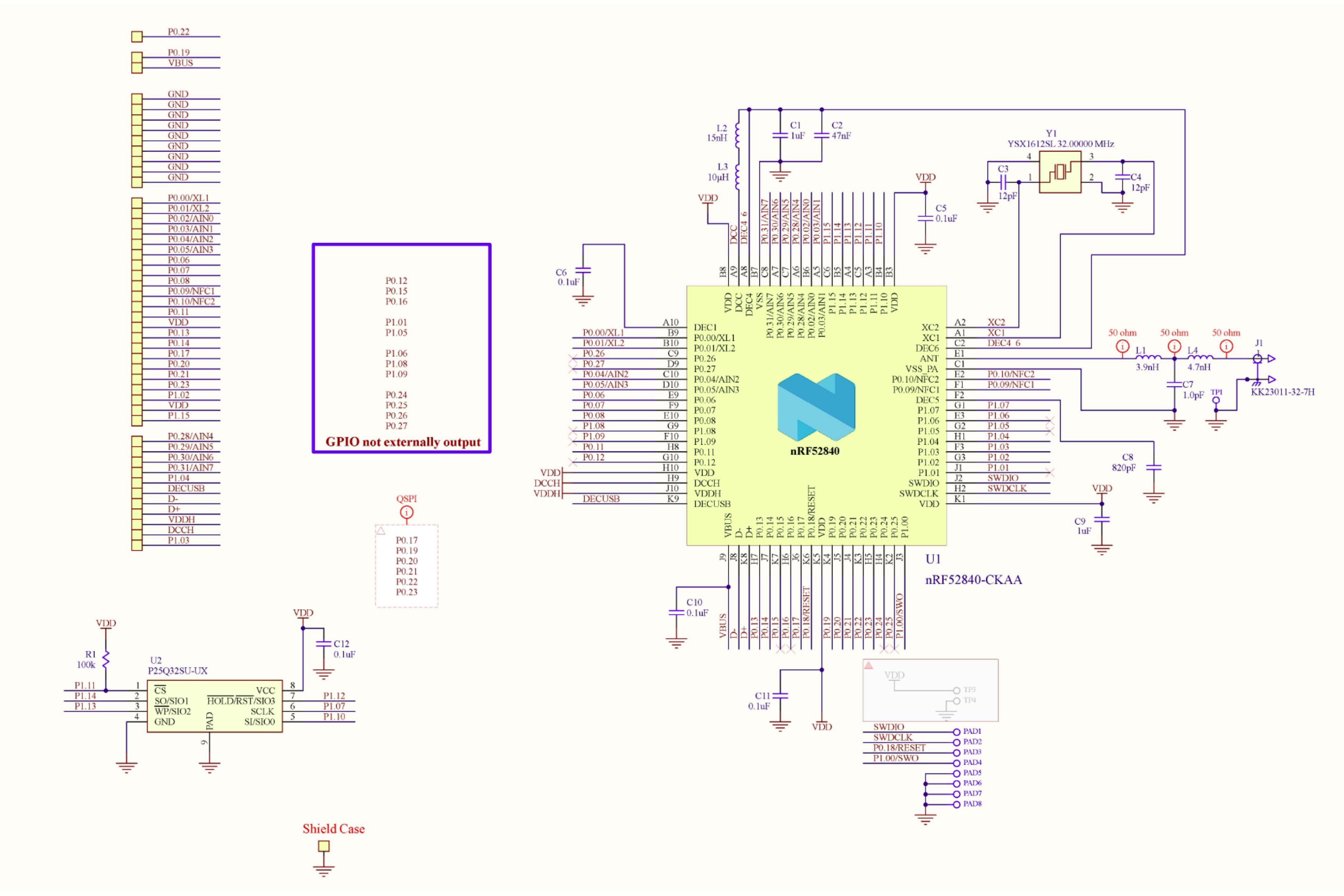
NX40i32